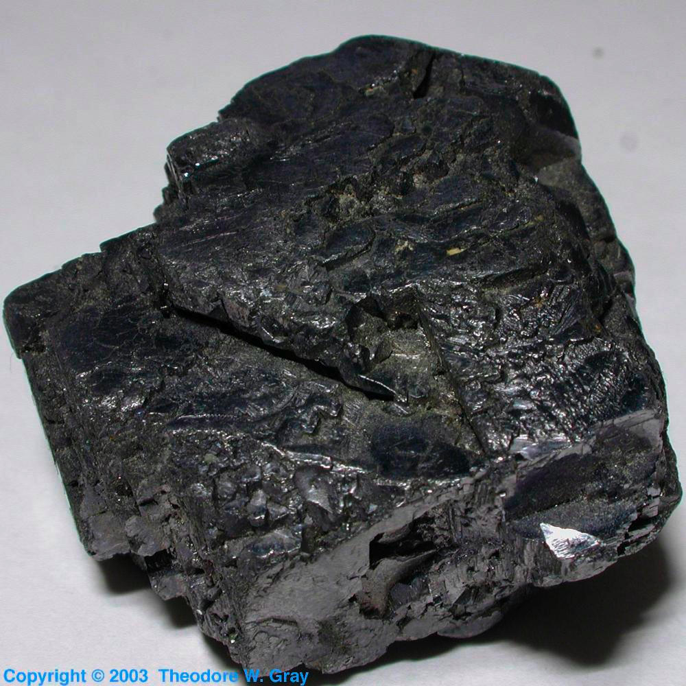
Lead Tin Sulfide (PbSnS₂)
Ternary Chalcogenide Semiconductor with Tunable Bandgap
MOQ: 100 Kilograms
Product Description
Lead Tin Sulfide (PbSnS₂) is a ternary chalcogenide semiconductor that enables precise bandgap tuning for specialized optoelectronic applications. This material system combines lead, tin, and sulfur to create a versatile semiconductor platform ideal for next-generation solar cells and infrared photodetectors.
The ability to adjust the lead-to-tin ratio allows engineers to optimize the material's electronic properties for specific wavelength requirements and device architectures. With decomposition temperatures above 700°C and excellent chemical stability under ambient conditions, PbSnS₂ supports standard semiconductor manufacturing processes while delivering performance characteristics competitive with more established technologies.
Key Features
- Tunable Bandgap: Adjustable from 1.3 eV to 1.8 eV through composition control
- High Absorption Coefficient: Exceeds 10⁴ cm⁻¹ above bandgap, enabling thin-film designs
- Thermal Stability: Chemically stable to 700°C, supporting standard fabrication processes
- Versatile Processing: Compatible with sputtering, spray pyrolysis, and electrodeposition
- Earth-Abundant Elements: No indium, gallium, or tellurium requirements
- Dual Conductivity Type: Can be engineered for n-type or p-type behavior
Primary Applications
Solar Energy Systems
PbSnS₂ serves as an absorber material in thin-film and quantum dot-sensitized solar cells. The tunable bandgap enables optimization to the ideal 1.5 eV range for solar energy conversion, achieving higher theoretical efficiencies than fixed-bandgap alternatives. Lead doping in tin sulfide reduces the optical bandgap from approximately 1.73 eV to 1.64 eV, positioning the material closer to the theoretical optimum for single-junction photovoltaic devices.
Infrared Photodetectors
The material's tunable response across visible and infrared spectral ranges makes it valuable for specialized imaging and sensing applications. The direct bandgap nature enables fast response times and high detectivity in photodetector configurations.
Thermoelectric Devices
The layered crystal structure and complex defect chemistry provide favorable combinations of electrical conductivity and thermal conductivity for energy harvesting applications.
Industrial Alloys
High-purity forms are used in soldering and brazing applications where thermal stability and controlled melting behavior are required.
Handling and Safety
- Toxicity Classification: Contains lead; handle as poisonous material
- Personal Protection: Gloves, safety glasses, and respiratory protection required when generating dust
- Storage: Sealed containers at room temperature, away from incompatible substances
- Processing: Use fume hoods with appropriate filtration
- Regulatory Compliance: Observe local occupational exposure limits for lead compounds